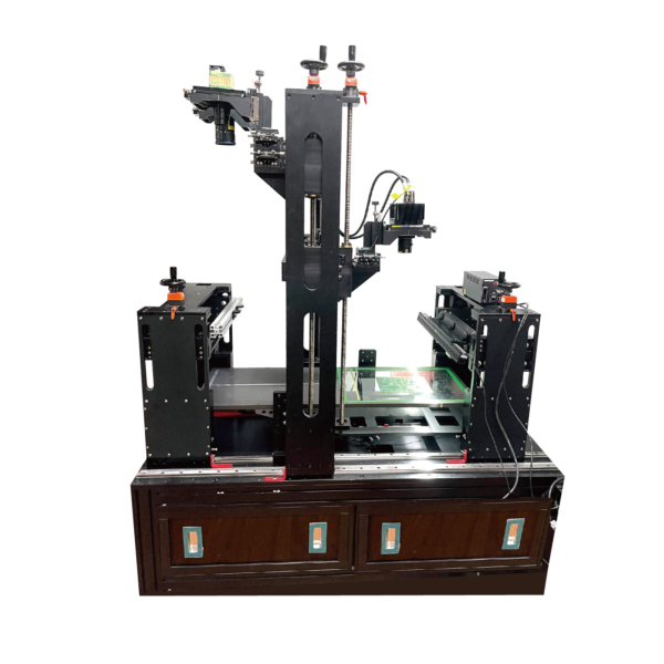
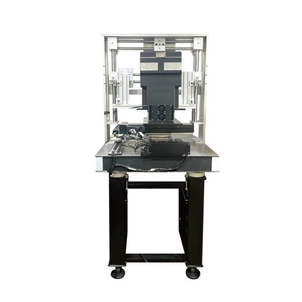
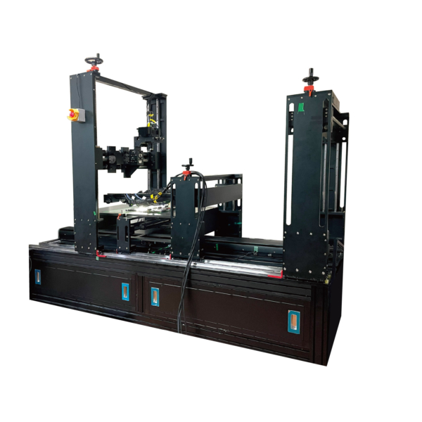
•Suitable for high-magnification line scans and area flying shots •Suitable applications: Wafer, IC in tray, Micro/Mini LED panel… •Maximum size of the object to be tested: 400mm(W)*500mm(L)